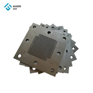
Advanced ceramic coatings, including SIC COATING and CVD SIC COATING, have revolutionized 300mm silicon wafer processing by addressing critical challenges in semiconductor manufacturing. Their exceptional thermal stability ensures reliable performance under extreme conditions. For instance, Kyocera’s plasma-resistant alumina ceramics exhibit less than 0.1% weight loss after 100 hours of exposure to CF₄/O₂ plasma. Chemical resistance further enhances the durability of these coatings, as noted in industry reports highlighting their growing demand in semiconductor applications. Innovations such as TAC COATING and CVD TAC COATING provide unmatched wear protection, ensuring equipment longevity. These advanced properties enable manufacturers to achieve higher precision, efficiency, and reliability in next-generation processes, solidifying Ningbo VET Energy Technology Co., Ltd’s commitment to cutting-edge solutions.
Key Takeaways
- Advanced ceramic coatings make 300mm silicon wafer tools last longer. They also help them work well in tough conditions.
- These coatings help factories work better by needing less fixing. They also lower mistakes, which means more good products are made.
- Using ceramic coatings saves money over time. They make tools last longer and need fewer repairs or replacements.
- New ideas like nanotechnology are improving ceramic coatings. These coatings are now thinner and work better for future uses.
- Ningbo VET Energy Technology Co., Ltd leads in making better ceramic solutions. They meet the changing needs of the chip-making industry.
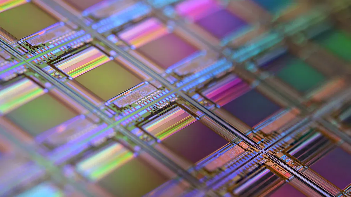
Importance of 300mm Silicon Wafer Processing

The Role of 300mm Silicon Wafers in Semiconductor Manufacturing
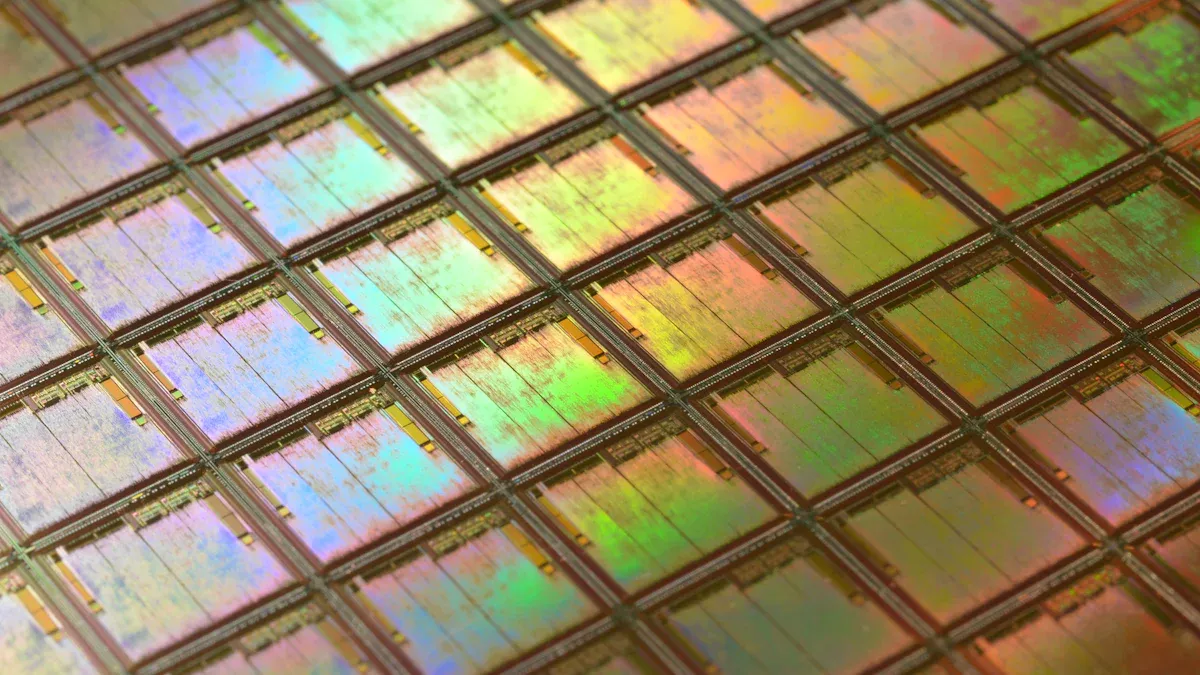
300mm silicon wafers have become the cornerstone of modern semiconductor manufacturing. Their larger size allows for the production of more chips per wafer, significantly improving cost efficiency and yield. This shift towards larger wafers aligns with the industry’s demand for advanced technologies like 5G, IoT, and AI.
The growing importance of 300mm wafers is evident in market trends.
- In 2023, these wafers accounted for 65% of total wafer production, showcasing their dominance.
- The global wafer market is projected to grow from approximately USD 10 billion in 2023 to USD 18 billion by 2032, driven by consumer electronics and automotive sectors.
Technological advancements such as EUV lithography and 3D packaging further enhance the capabilities of 300mm wafers. These innovations enable manufacturers to meet the increasing demand for high-performance and energy-efficient devices. Additionally, outsourcing trends among fabless semiconductor firms have created new opportunities for foundries specializing in 300mm wafer production.
| Evidence Type | Description |
|---|---|
| Market Share | Increasing demand for larger wafer sizes, particularly 300mm and beyond. |
| Technological Advancements | EUV lithography and 3D packaging drive growth in semiconductor manufacturing. |
| Outsourcing Trends | Fabless firms outsourcing wafer production to foundries for efficiency. |
Challenges in Processing Larger Wafers
Despite their advantages, processing 300mm wafers presents unique challenges. The transition from smaller wafers, such as 200mm, requires significant investment and expertise. Startup costs for 300mm wafer fabs exceed $15 billion, making them a high-risk venture.
| Aspect | 200mm Wafer | 300mm Wafer |
|---|---|---|
| Startup Costs | Lower | Very high (>$15 billion) |
| Technical Expertise | Moderate | Significantly higher |
| Process Development Complexity | Lower | Substantially increases |
Manufacturing complexity also rises with larger wafers. Advanced lithography, bonding, and etching technologies are essential to maintain precision. Yield management becomes critical, as defects in a single wafer can impact multiple integrated dies. This necessitates advanced detection and improvement techniques to minimize losses.
Additionally, the need for automation in 300mm wafer processing has led to increased outsourcing. While this improves efficiency, it also complicates supply chains, especially during economic instability. Trade wars and global dependencies further exacerbate these challenges.
“The operational cost of 300mm wafer production is significantly greater than that of 200mm fabs. Real-time monitoring of product can save time and money through reduced scrap and decreased cycle time.”
Ceramic coatings play a vital role in addressing these challenges. Their exceptional durability and thermal stability ensure reliable performance in advanced wafer processing equipment, supporting the industry’s transition to larger wafers.
Ceramic Coatings in Wafer Processing
Key Properties of Ceramic Coatings
Ceramic coatings exhibit a unique combination of properties that make them indispensable in 300mm silicon wafer processing. Their exceptional thermal stability allows them to withstand extreme temperatures, ensuring reliable performance in high-heat environments. This characteristic is particularly critical in processes like chemical vapor deposition (CVD) and physical vapor deposition (PVD), where temperatures can exceed 1000°C. Additionally, ceramic coatings offer superior chemical resistance, protecting equipment from corrosive gases and liquids commonly used in semiconductor manufacturing.
Durability and wear resistance are other defining features of ceramic coatings. These coatings maintain their structural integrity under mechanical stress, reducing equipment downtime and maintenance costs. Various testing methods have been established to evaluate these properties:
| Testing Method | Description |
|---|---|
| Taber Abrasion | Determines a material’s resistance to abrasion, indicating how well it withstands mechanical actions. |
| Micro-abrasion Technique | Allows precise study of surface wear, isolating the effects of test conditions on wear resistance. |
| Pin-on-Disk Wear Testing | Used for tribological characterization, estimating friction and wear mechanisms between materials. |
| RCA Wear Testing | Tests surfaces for abrasion resistance, commonly used in various industries for different materials. |
| Blade-on-Block Wear Testing | Characterizes properties like lifespan of coatings and coefficient of friction through specific testing. |
These advanced properties ensure that ceramic coatings can endure the rigorous demands of next-generation wafer processing, enhancing both efficiency and reliability.
Applications in Wafer Fabrication Equipment
Ceramic coatings play a pivotal role in the performance and longevity of wafer fabrication equipment. Their ability to provide high thermal conductivity and electrical insulation makes them ideal for critical components in semiconductor manufacturing. Plasma-sprayed alumina, for instance, is widely used in PVD and CVD chambers due to its excellent thermal and electrical properties. Similarly, plasma-sprayed aluminum oxide coatings offer high dielectric strength and thermal shock resistance, making them suitable for high-temperature applications.
The following table highlights specific applications of ceramic coatings in wafer fabrication equipment:
| Ceramic Coating Type | Key Benefits | Applications in Wafer Fabrication Equipment |
|---|---|---|
| Plasma Sprayed Alumina | High thermal conductivity, withstands high temperatures, excellent electrical properties | Used in PVD and CVD chambers for insulation |
| Plasma Sprayed Aluminum Oxide | High dielectric strength, superior thermal shock resistance | Ideal for semiconductor manufacturing equipment |
| Plasma Spray Yttrium Oxide | Increased resistance to thermal cycling, improved dielectric strength | Suitable for various semiconductor processes |
| Cubic Silicon Carbide | High temperature resistance in various gases | Used in MOCVD, CVD, PECVD, and PVD processes |
In addition to these applications, ceramic coatings significantly reduce chemical contamination in processing equipment. For example:
- Alumina coatings maintain structural integrity across a wide pH range, outperforming traditional zinc-rich coatings.
- Pharmaceutical manufacturers using alumina-coated reactors report a 50% decrease in contamination incidents compared to stainless steel surfaces.
- Offshore oil platform components with alumina coatings experience a 70% reduction in saltwater corrosion damage.
These examples underscore the versatility and effectiveness of ceramic coatings in enhancing the performance and durability of wafer fabrication equipment. Ningbo VET Energy Technology Co., Ltd continues to lead the industry by developing advanced ceramic solutions tailored to the evolving demands of semiconductor manufacturing.
Benefits of Ceramic Coatings in Semiconductor Manufacturing
Enhancing Process Efficiency and Yield
Ceramic coatings significantly enhance the efficiency and yield of semiconductor manufacturing processes. Their exceptional thermal stability ensures consistent performance in high-temperature environments, such as chemical vapor deposition (CVD) and physical vapor deposition (PVD). This stability minimizes thermal fluctuations, which can lead to defects in wafer production. By maintaining precise temperature control, ceramic coatings help manufacturers achieve higher yields with fewer rejected wafers.
The chemical resistance of ceramic coatings also plays a critical role in improving process efficiency. These coatings protect equipment from corrosive gases and chemicals used during wafer fabrication. This protection reduces the frequency of equipment maintenance and cleaning, allowing for uninterrupted production cycles. For example, plasma-sprayed alumina coatings are widely used in CVD chambers to prevent chemical contamination, ensuring a cleaner and more efficient manufacturing environment.
Additionally, ceramic coatings contribute to better yield management by reducing the risk of defects caused by wear and abrasion. Their durability ensures that critical components, such as wafer carriers and chamber walls, maintain their structural integrity over extended periods. This reliability translates into fewer production disruptions and higher overall efficiency.
Improving Durability and Reducing Costs
The durability of ceramic coatings offers substantial cost-saving benefits in semiconductor manufacturing. These coatings extend the lifespan of wafer fabrication equipment by protecting it from mechanical wear, thermal stress, and chemical corrosion. This longevity reduces the need for frequent replacements and repairs, leading to significant long-term savings.
Investing in ceramic coatings proves to be a financially sound decision when considering their impact on maintenance costs. Traditional protective solutions, such as polymer coatings, require frequent reapplications, increasing operational expenses. In contrast, ceramic coatings provide long-lasting protection, often lasting several years with minimal upkeep. For instance, while the initial cost of applying ceramic coatings may be higher, the reduced maintenance requirements and extended equipment lifespan result in lower overall expenses.
Comparative economic studies highlight the cost advantages of ceramic coatings over alternative solutions. Traditional protective methods, such as wax coatings, demand regular reapplications, leading to repetitive costs. Ceramic coatings, on the other hand, can last 2 to 5 years, significantly reducing maintenance expenses. For example, a high-quality ceramic coating may cost $1,000 initially but provides years of protection, translating to an annual cost of just $200. In contrast, spending $50 monthly on alternative solutions results in an annual cost of approximately $600, showcasing the financial benefits of ceramic coatings.
Moreover, the enhanced durability of ceramic coatings contributes to the resale value of manufacturing equipment. By maintaining the equipment’s condition and performance, these coatings ensure that it retains its value over time. This preservation not only benefits manufacturers during resale but also supports their long-term financial planning.
Ningbo VET Energy Technology Co., Ltd continues to lead the industry by developing advanced ceramic solutions that address the evolving demands of semiconductor manufacturing. Their innovative coatings deliver unmatched durability and cost efficiency, empowering manufacturers to optimize their operations and achieve sustainable growth.
Innovations in Ceramic Coatings
Emerging Coating Technologies for Wafer Processing
The rapid evolution of semiconductor manufacturing has spurred significant advancements in ceramic coating technologies. Researchers are leveraging nanotechnology to develop thinner, more efficient coatings with enhanced thermal and chemical properties. These innovations enable precise control over coating thickness, improving performance in high-temperature environments. Multifunctional coatings are also gaining traction, offering combined benefits such as corrosion resistance and thermal management. This dual functionality reduces the need for multiple layers, streamlining manufacturing processes.
Customization has become a key focus, with manufacturers tailoring ceramic coatings to meet specific requirements. For instance, coatings with adjustable surface roughness are now available, allowing for optimized performance in wafer processing equipment. Continuous investment in research and development drives these advancements, ensuring that ceramic coatings remain at the forefront of semiconductor innovation.
| Trend | Description |
|---|---|
| Use of Nanotechnology | Leveraging nanotechnology to create thinner, more efficient coatings with enhanced properties. |
| Development of Multifunctional Coatings | Creating coatings that provide multiple functions like corrosion protection and thermal management. |
| Customization of Coatings | Offering tailored coatings to meet specific needs of semiconductor manufacturers. |
| Increase in Research and Development | Continuous investment in R&D driving innovative product development for high-performance coatings. |
Ultra-high-temperature ceramic coatings (UHTCCs) are particularly noteworthy. These coatings exhibit exceptional thermal stability, withstanding temperatures up to 1600°C. Their ability to endure extreme conditions makes them indispensable for high-precision applications in AI, autonomous vehicles, and 5G technologies. As electronic devices become more compact and operate at higher speeds, the demand for UHTCCs continues to grow, driven by advancements in electric vehicles and sustainable manufacturing practices.
Adapting to Next-Gen Manufacturing Demands
The semiconductor industry faces increasing pressure to adapt to next-generation manufacturing demands. Ceramic coatings play a pivotal role in meeting these challenges by enhancing the performance and durability of wafer processing equipment. High-purity coatings, for example, ensure minimal contamination during fabrication, a critical requirement for advanced technologies like EUV lithography.
Emerging ceramic coatings also offer exceptional coverage, even on complex shapes, ensuring comprehensive protection. Their corrosion resistance and thermal stability make them ideal for reactive environments, where traditional materials often fail. These properties align with the industry’s shift toward eco-friendly and durable solutions, particularly in sectors like aerospace, automotive, and renewable energy.
| Key Property | Description |
|---|---|
| Maximum Operating Temperature | Up to 1600°C, ensuring reliability in high-temperature environments. |
| Corrosion Resistance | Exceptional protection against corrosion in reactive environments. |
| Thermal Stability | Maintains structural integrity at high temperatures. |
| Customizable Surface Roughness | Allows for tailored applications based on specific needs. |
| High Purity Coating | Enhances performance in semiconductor manufacturing and other applications. |
| Exceptional Coverage | Effective on complex shapes, ensuring comprehensive protection. |
Industry analysis highlights the adaptability of ceramic coatings across various applications. In solar panel manufacturing, these coatings protect against corrosion and staining, enhancing durability in harsh conditions. Aerospace components benefit from their high-temperature resistance, improving engine efficiency. The automotive sector also sees growth in advanced coatings, driven by the demand for eco-friendly and long-lasting solutions.
- Increasing use of transparent conductive coatings in solar technology.
- Application in aerospace for high-efficiency engines.
- Growth in advanced coatings driven by eco-friendly and durable solutions.
Ningbo VET Energy Technology Co., Ltd remains at the forefront of these innovations, offering cutting-edge ceramic solutions tailored to the evolving needs of next-generation manufacturing.
Advanced ceramic coatings have become essential in addressing the complexities of 300mm silicon wafer processing. Their unique properties, such as thermal stability and chemical resistance, ensure superior efficiency, durability, and precision in semiconductor manufacturing. These coatings not only meet current industry demands but also pave the way for future innovations in high-performance technologies.
As a leader in advanced ceramic solutions, Ningbo VET Energy Technology Co., Ltd continues to drive progress by delivering cutting-edge coatings tailored to next-generation applications. Their commitment to innovation positions them at the forefront of the semiconductor industry.
FAQ
What makes ceramic coatings essential for 300mm silicon wafer processing?
Ceramic coatings provide unmatched thermal stability, chemical resistance, and wear protection. These properties ensure reliable performance in high-temperature and corrosive environments, making them indispensable for advanced semiconductor manufacturing processes like CVD and PVD.
How do ceramic coatings improve wafer fabrication equipment?
Ceramic coatings enhance equipment durability by protecting against mechanical wear, thermal stress, and chemical corrosion. This protection reduces maintenance needs, minimizes downtime, and extends the lifespan of critical components, ensuring consistent performance in wafer processing.
Are ceramic coatings cost-effective for semiconductor manufacturing?
Yes, ceramic coatings offer long-term cost savings. Their durability reduces the frequency of equipment repairs and replacements. Although the initial application cost may be higher, the extended lifespan and reduced maintenance expenses make them a financially sound investment.
What innovations are shaping the future of ceramic coatings?
Emerging technologies like nanotechnology and ultra-high-temperature ceramic coatings (UHTCCs) are transforming the industry. These advancements enable thinner, multifunctional coatings with enhanced thermal and chemical properties, meeting the demands of next-generation semiconductor manufacturing.
How does Ningbo VET Energy Technology Co., Ltd contribute to the industry?
Ningbo VET Energy Technology Co., Ltd leads the development of advanced ceramic solutions. Their innovative coatings address the evolving challenges of semiconductor manufacturing, ensuring superior efficiency, durability, and precision for next-generation applications.