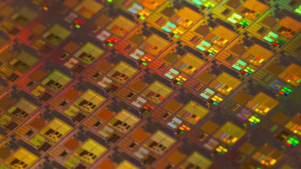
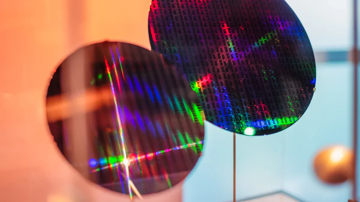
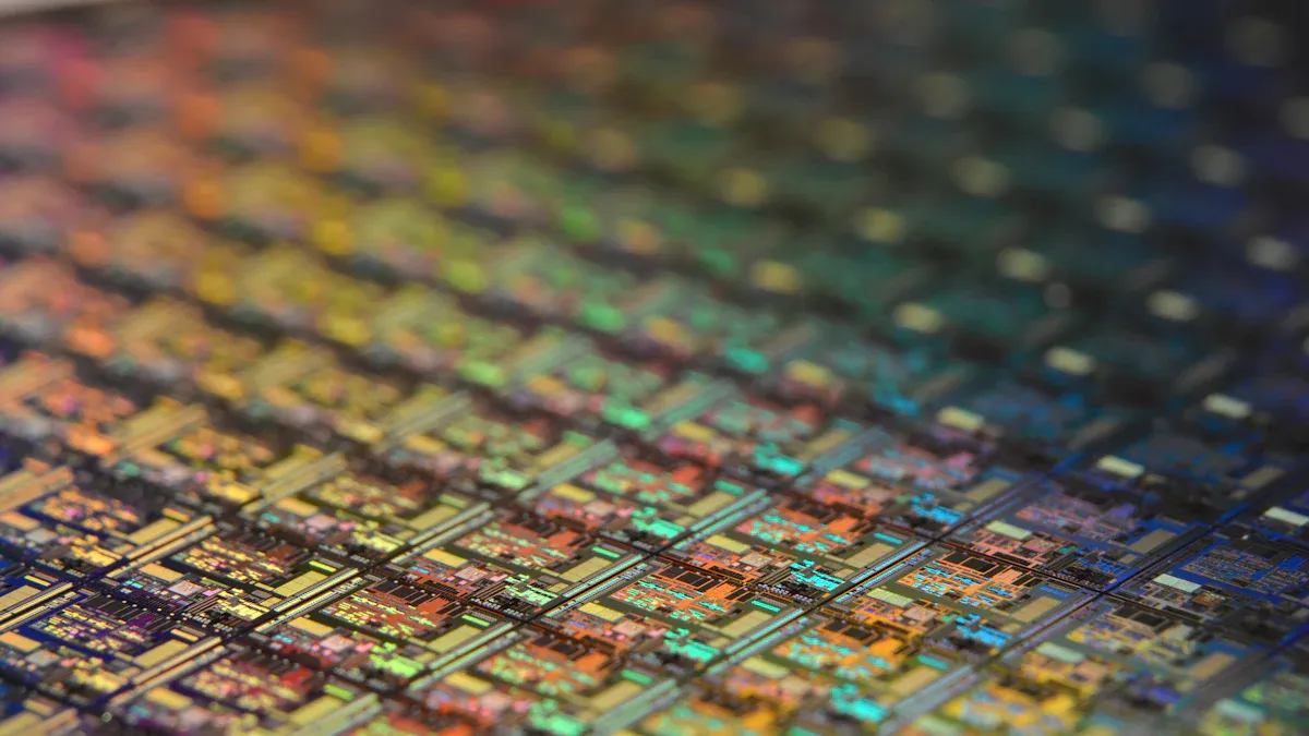
Semiconductor wafer handling requires exceptional precision and reliability. CVDコーティング services fulfill these requirements by forming protective layers that enhance durability and minimize contamination. Advanced materials such as SIC COATING and TAC COATING play a crucial role in improving wafer surfaces, reducing risks during the fabrication process. Specifically, CVD SIC COATING and CVD TAC COATING provide enhanced solutions for optimizing handling tools, ensuring consistent and reliable performance in both research and production settings. These coatings deliver outstanding chemical and thermal stability, empowering manufacturers to scale their operations with confidence and efficiency.
要点
- CVDコーティング makes wafer tools last longer by reducing damage. This means tools need replacing less often, saving money.
- It adds protective layers that stop contamination, leading to better production and fewer mistakes in making semiconductors.
- CVD Coating handles heat and chemicals well, so tools stay strong in tough conditions and work reliably.
- Using advanced materials and machines in CVD Coating makes it faster and more accurate, improving quality and cutting waste.
- Adding AI to CVD Coating helps improve production, checks tools better, and saves energy to support the environment.
Challenges in Semiconductor Wafer Handling
Semiconductor wafer handling presents several challenges that manufacturers must address to ensure efficiency and profitability. These challenges become more pronounced during the transition from research and development (R&D) to mass production, where precision and consistency are critical.
Contamination Risks in R&D and Production
Contamination remains one of the most significant risks in wafer handling. Manufacturers must control process variables meticulously to prevent foreign material from disrupting functionality. Even trace contaminants can lead to production interruptions and increased costs. For example, the purity of chemicals used in post-etch residue removal must be characterized to parts-per-trillion levels. Any deviation can compromise the integrity of advanced integrated circuits.
注: A single raw wafer costs approximately $500, and finished wafers for high-end processors can exceed $5000. Contamination at any stage can result in substantial financial losses, especially in large fabrication plants processing up to 50,000 wafers monthly.
To mitigate contamination risks, the semiconductor industry invests heavily in precise materials characterization and advanced cleaning protocols. These measures enhance manufacturing predictability and reduce the likelihood of defects.
Handling Fragile Wafers During Scaling
Scaling operations from R&D to production introduces challenges in handling fragile wafers. These wafers undergo over 1000 process steps, making them susceptible to physical damage such as chips, cracks, or microcracks. Such defects can render wafers unusable, significantly impacting yield.
Manufacturers employ specialized tools and techniques to minimize physical damage. For instance, wafer handling systems equipped with CVDコーティング improve surface durability, reducing the risk of mechanical stress during transport and processing. Enhanced durability ensures that wafers remain intact throughout the production cycle, supporting higher yields and profitability.
Process Variability in Mass Production
Process variability is another critical challenge in semiconductor manufacturing. Variations in process steps can significantly impact wafer quality, yield, and profitability. Each step is governed by a detailed process of record, including chemical composition and impurity levels. Deviations from these records can lead to defects and reduced efficiency.
To address variability, manufacturers rely on advanced measurement techniques. These include:
- Defect Density Measurement (DDM): Counts flaws per unit area, indicating manufacturing efficiency.
- Microcrack Detection: Identifies microcracks that could lead to wafer failure.
- Thickness Measurement: Evaluates wafer thickness and total thickness variation using capacitance techniques.
- Photoluminescence Imaging: Detects efficiency-limiting defects, especially in multicrystalline silicon wafers.
| Measurement Technique | 説明 |
|---|---|
| Final Inspection and Testing | Ensures wafers meet specifications, including electrical functionality and reliability under conditions. |
| Bulk Resistivity Check | Assesses resistivity using non-contact eddy current techniques. |
| 2D Geometric Inspection | Checks for chips or large cracks, discarding imperfect wafers. |
By implementing these techniques, manufacturers can reduce variability and ensure consistent wafer quality. CVD Coating further enhances wafer stability, providing thermal and chemical resistance that supports reliable performance during mass production.
Benefits of CVD Coating in Wafer Handling
耐久性と寿命の向上
CVD Coating significantly enhances the durability and lifespan of wafer handling tools and equipment. By forming a robust protective layer, these coatings shield surfaces from wear and tear caused by repeated use in high-stress environments. For example, quenching sleeves coated with CVD materials at Samsung Austin demonstrated remarkable performance improvements. Unlike uncoated equipment that degraded quickly, the coated sleeves operated efficiently for over 70 days without failure. This extended lifespan reduces the frequency of replacements, minimizing downtime and operational costs.
The enhanced durability also supports environmental sustainability. Longer-lasting equipment means fewer discarded parts, aligning with the industry’s goals to reduce waste and promote eco-friendly practices. Additionally, the improved resistance to corrosion and mechanical stress ensures that tools maintain their functionality even under demanding conditions, contributing to higher yields in semiconductor production.
Reduction in Contamination and Defects
Contamination poses a critical challenge in semiconductor manufacturing, but CVD Coating effectively mitigates this risk. The coatings create a barrier that prevents the release of particles and metal ions, which can compromise wafer integrity. This reduction in contamination directly translates to fewer defects and higher production yields.
Statistical data highlights the transformative impact of CVD Coating on contamination control:
| Improvement Type | Before CVD Coating | After CVD Coating | Percentage Change |
|---|---|---|---|
| Boat Lifespan (times) | 300 | 5000 | 1566.67% |
| Annual Maintenance Cost Reduction | N/A | 62% | N/A |
| Diffusion Furnace Tube Lifespan | N/A | 3 times | N/A |
These improvements not only enhance operational efficiency but also reduce maintenance costs. By minimizing contamination, manufacturers can achieve consistent wafer quality, ensuring that each production cycle meets stringent industry standards.
Improved Thermal and Chemical Stability
Semiconductor manufacturing involves extreme thermal and chemical conditions that can degrade unprotected surfaces. CVD Coating provides exceptional thermal and chemical stability, enabling tools and equipment to withstand these harsh environments. The coatings act as a protective shield, preventing chemical reactions that could damage surfaces or introduce impurities.
For instance, the enhanced corrosion resistance offered by CVD Coating ensures that equipment remains functional even when exposed to aggressive chemicals used in wafer processing. This stability is crucial for maintaining the precision and reliability required in semiconductor fabrication. Furthermore, the coatings’ ability to endure high temperatures without degradation supports consistent performance across various production stages.
By improving thermal and chemical stability, CVD Coating enables manufacturers to optimize their processes, reduce downtime, and achieve higher yields. This technological advantage plays a pivotal role in advancing semiconductor production from R&D to large-scale manufacturing.
Applications of CVD Coating in Semiconductor Manufacturing
Cleanroom Equipment and Wafer Handling Tools
Cleanroom environments demand tools that resist contamination and wear. CVDコーティング enhances the durability and cleanliness of wafer handling tools, such as tweezers, carriers, and robotic arms. These coatings create a non-reactive surface that minimizes particle generation and prevents chemical interactions. This improvement ensures that wafers remain pristine during transport and processing.
Samsung Austin’s application of CVD coatings on quenching sleeves illustrates this benefit. The coated sleeves operated efficiently for over 70 days without degradation, while uncoated equipment failed much sooner. This advancement reduced contamination risks, extended equipment lifespan, and lowered replacement costs. By adopting CVD-coated tools, manufacturers can maintain cleanroom standards and improve operational efficiency.
Gas Delivery and Deposition Systems
Gas delivery systems play a critical role in semiconductor manufacturing, particularly during chemical vapor deposition processes. CVD coating enhances the performance of these systems by providing chemical resistance and thermal stability. Coated surfaces prevent corrosion caused by reactive gases, ensuring consistent flow and deposition quality.
Manufacturers benefit from reduced maintenance and downtime, as coated components withstand harsh conditions without degradation. This reliability supports precise gas delivery, which is essential for achieving uniform thin film deposition. By integrating CVD-coated components into gas delivery systems, facilities can optimize production cycles and maintain high yields.
Etching and Thin Film Deposition Processes
Etching and thin film deposition processes expose equipment to aggressive chemicals and extreme temperatures. CVD coating protects these surfaces, enabling tools to endure repeated exposure without losing functionality. The coatings act as a barrier, preventing chemical reactions that could compromise equipment integrity or introduce impurities into the wafer.
For example, diffusion furnace tubes coated with CVD materials exhibit extended lifespans, reducing the frequency of replacements. This improvement minimizes downtime and supports continuous production. Additionally, the enhanced thermal stability of CVD-coated surfaces ensures consistent performance during high-temperature processes, contributing to better wafer quality and higher yields.
Innovations in CVD Coating Technology
Advanced Materials for High-Performance Coatings
The development of advanced materials has revolutionized the efficiency of CVD Coating in semiconductor manufacturing. These materials enhance coating performance by improving durability, chemical resistance, and thermal stability. For instance, materials like BPSG, Draco™, and Pioneer CVD have demonstrated remarkable advancements in coating efficiency.
| 素材 | Impact on CVD Efficiency | Year Introduced |
|---|---|---|
| BPSG | Used for gap fill in DRAM, still in production today | 1995 |
| Draco™ | Increases etch selectivity by over 30% | 2021 |
| Pioneer CVD | More resilient to etch chemistries, allows thinner stacks | 最近 |
These innovations enable manufacturers to achieve higher yields and reduce defects, ensuring consistent wafer quality during production.
Automation and Precision in Coating Application
Automation has become a cornerstone of modern CVD Coating processes. Advanced control systems now allow real-time monitoring and adjustment of deposition parameters, ensuring precise and uniform coatings. This level of precision minimizes material waste and enhances overall efficiency.
Technological advancements in automation and control systems enhance the precision and efficiency of the coating process. Real-time monitoring technologies enable manufacturers to optimize deposition rates and material properties, leading to superior coating quality.
Statistical process control (SPC) methods further refine the process by analyzing data and maintaining tighter tolerances. These innovations reduce variability, ensuring that every wafer meets stringent industry standards.
Integration with AI and Industry 4.0
The integration of AI and Industry 4.0 technologies has unlocked new possibilities for optimizing CVD Coating applications. AI-driven systems now monitor deposition processes, adjust parameters in real time, and improve material efficiency.
| 応用分野 | AI Technique Used | ベネフィット |
|---|---|---|
| Real-time Parameter Optimization | Reinforcement Learning | Adjusts parameters like precursor flow rate and plasma power to meet specifications |
| Monitoring | AI-driven Virtual Sensors | Enhances monitoring of deposition processes for improved quality control |
| Production Coordination | Multi-Agent Systems | Coordinates production processes to reduce waste and improve efficiency |
| Material Efficiency | AI Models | Optimizes precursor usage to minimize wastage during deposition cycles |
| 環境への影響 | AI-driven Simulations | Identifies low-energy pathways for chemical reactions, reducing carbon footprint |
These advancements not only improve production efficiency but also align with sustainability goals by reducing waste and energy consumption.
CVDコーティング has transformed semiconductor manufacturing by addressing critical wafer handling challenges. Its ability to enhance durability, reduce contamination, and improve thermal stability ensures consistent performance from R&D to production. Manufacturers have increasingly adopted this technology, with 78% of dielectric layer applications now utilizing CVD-processed silicon nitride films. This shift has reduced dielectric breakdowns by 40% during accelerated life testing, demonstrating its reliability. Furthermore, its compatibility with high-k materials like hafnium oxide resolves leakage current issues in advanced logic gates. Exploring advancements in CVD technology will unlock further efficiencies and innovations in semiconductor fabrication.
よくあるご質問
What is CVD coating, and why is it important in semiconductor manufacturing?
CVD (Chemical Vapor Deposition) coating is a process that deposits thin films onto surfaces using chemical reactions. It enhances the durability, thermal stability, and contamination resistance of tools and wafers, ensuring consistent performance during semiconductor fabrication.
How does CVD coating reduce contamination in wafer handling?
CVD coatings create non-reactive, protective layers that prevent particle generation and chemical interactions. This barrier minimizes contamination risks, leading to fewer defects and higher production yields in semiconductor manufacturing.
Can CVD coatings withstand extreme temperatures and chemicals?
Yes, CVD coatings provide exceptional thermal and chemical stability. They protect surfaces from degradation caused by high temperatures and aggressive chemicals, ensuring reliable performance throughout the semiconductor production process.
What tools in semiconductor manufacturing benefit from CVD coatings?
CVD coatings enhance the performance of wafer handling tools, cleanroom equipment, gas delivery systems, and etching components. These coatings improve durability, reduce maintenance needs, and ensure contamination-free operations.
Are CVD coatings environmentally friendly?
CVD coatings contribute to sustainability by extending the lifespan of tools and reducing waste. Their durability minimizes the frequency of replacements, aligning with the industry’s eco-friendly goals.