について シリコンウェーハ製造工程 原材料を高品質のシリコンウェーハに変換し、現代の電子機器に不可欠です。 砂から抽出されたシリコンで始まり、 不純物を取除く浄化. . 浄化されたケイ素は溶解し、インゴットに形づけられます。 これらのインゴットは薄いsiのウエファーにスライスされ、滑らかさのために磨かれ、汚染物質を取除くためにきれいにされます。 各ステップは保障します シリコンウエハ 半導体アプリケーションに必要な高い基準を満たし、信頼性のある作業に不可欠です シリコンウェーハサプライヤー.
シリコンウェーハの原料の調製
シリコンの浄化
シリコンウェーハを作成する旅は、第一次原料であるシリカ砂から始まります。 この砂は最終製品の品質を確保するために厳格な純度基準を満たしなければなりません。 あなたは、中国、ロシア、ブラジル、米国を含む様々な国からシリカ砂が供給されていることを学ぶために驚くかもしれません。 収集したら、砂は鉄およびアルミニウムのような不純物を取除くために浄化プロセスを経ます。 このステップは、トレースの汚染物質であっても、電子機器のシリコンウェーハの性能に影響を与える可能性があるため重要です.
精製された無水ケイ酸は高温減少プロセスによって冶金学等級のケイ素(MGS)にそれから変形します。 これは電気アーク炉のカーボンが付いている砂を熱することを含みます。 結果は、次の段階の基礎として機能する98-99%の純度のレベルを持つシリコンの固体形態です.
Polysiliconへの変換
電子機器に必要な超高純度を実現するために、冶金学位のシリコンはさらなる精製を受けています。 このプロセスは、シリコンを微細な粉末に粉砕することによって始まります。 パウダー 無水塩酸(HCl)と液化ベッド反応器で反応し、トリクロロシラン(SiHCl3)を生産. . この反応は次のように表現できますSi + 3HCl → SiHCl3 + H2
次に、トリクロロシランは、不純物を除去するための僅かな蒸留によって浄化されます。 精製コンパウンドをSiemensリアクターに導入し、高温での水素削減を実現します。 このステップは、ポリシリコンロッドを形成し、加熱シリコンフィラメントに高純度シリコンを堆積させます。 これらのロッドは、シリコンウェーハの生産の次のフェーズの準備ができて、後にチャンクに分解されます.
ニンポー VET エネルギー技術Co.、 ケイ素のような先端材料を専門にし、このプロセスのすべてのステップが最高水準を満たしていることを保障します。 最先端の半導体用途に適した材料の生産を保証します.
シリコンウェーハ製造における結晶成長

Czochralskiプロセス
Czochralskiプロセスは、高品質のシリコンウェーハの製造に重要な役割を果たしています。 この方式は性能および信頼性のために不可欠である例外的な純度の単一水晶ケイ素を作り出します 半導体デバイス. . 現代の電子機器の厳しい要求を満たしたウェーハを作成する基盤として考えられます.
このプロセスでは、小さな種子結晶を溶融シリコンに慎重に下げます。 皮膜の結晶が回転し、溶融シリコンが固着する。 この段階的な凝固は均一水晶構造の形成を保障します。 また、プロセスは、シリコンの電気特性をドーピングを介して正確に制御することができます, 特定の要素は、溶融シリコンに追加されます.
- Czochralskiプロセスはウエファーの生産で使用される成長するケイ素の水晶のための第一次方法です.
- それは一貫した質のウエファーに終って最低の不純物を保障します.
- 高度の電子適用のために達成される均一水晶構造は重要です.
ニンポー VET エネルギー技術Co.、 当社は、Czochralskiプロセスのような高度な技術を活用して、材料が最高の業界標準を満たしていることを確認します.
シングルクリスタルインゴットの形成
Czochralskiプロセスが完了すると、結果は単一のクリスタルインゴットです。 シリコンウェーハ製造工程のバックボーンを形成する円筒構造です。 インゴットの均等性は、ウェーハがそれからスライスしたことを一貫した電気的および物理的性質があることを保障します.
ひとつの結晶が重要なのはなぜだろうか。 単結晶構造で、半導体デバイスにおける電力の流れを破壊できる粒度を排除。 高性能電子機器に用いられるウェーハを作るためのインゴット理想です.
インゴットは、薄いウェーハにスライスされる前に、さらにシェーピングと準備を受けます。 各ステップは最終製品が半導体業界の厳しい要件を満たしていることを確認します。 寧波VETエネルギー技術有限公司、 高品質の素材を生産し、すべてのインゴットが信頼できるシリコンウェーハの作成に貢献できるようにする株式会社エクセル.
シリコンインゴットのシェーピングとスライス
インゴットの円筒形のシェーピング
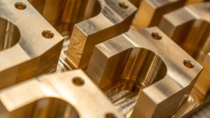
単一の水晶インゴットが形成されると、それを完全なシリンダーに形づける必要があります。 このステップは、高品質のシリコンウェーハを作成するために重要な均一性を保証します。 インゴットは、表面が滑らかで円筒状の形状を達成するために慎重に接地する旋盤の上に置かれます。 このプロセスは不規則性を取除き、正確なスライスのためのインゴットを準備します.
精度を高めるために、インゴットは「フラットまたはノッチマーク」と呼ばれるプロセスを受けています。 これは、シリンダーに沿って平らなエッジや小さなノッチを作成することを含みます。 ウェハースライシングや半導体製造後の段階におけるアライメントガイドとして機能します。 インゴットが完全に形づけられていることを確実にすることによって、一貫したウェーハ品質の基盤を置きます.
スライスする 薄いウエファー
シェーピング後、円筒インゴットは、先端切削技術を使用して薄手のウェーハにスライスされます。 精密はこのステップの間にキーです。 欠陥を避けるために切断プロセスの温度と速度を慎重に制御し、ウェーハの構造的完全性を維持する必要があります.
スライスプロセスは研摩のスラリーかダイヤモンド上塗を施してあるワイヤーが装備されているワイヤー ソーを使用します。 ウエファーが希望する厚さおよび表面質を達成するこの方法を保障します。 結果のウエハは、厚さミリ未満の非常に薄く、半導体アプリケーションに必要な強度を保持します.
- 精密達成の重要な要因は下記のものを含んでいます:
- 温度および切断の速度の有用な制御.
- 欠陥を最小限に抑える高度な切削技術.
- 最適性能のための一貫した厚さそして質.
ニンポー VET エネルギー技術Co.、 あらゆるシリコンウェーハが最も高い業界基準を満たしていることを確認するために、最先端技術を採用しています。 同社の専門知識は、ウェーハを優れた精度と信頼性で保証し、高度な電子機器に最適です.
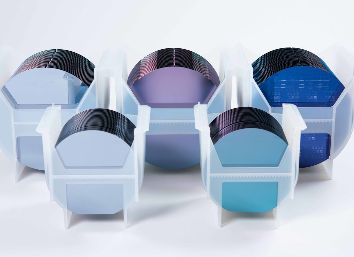
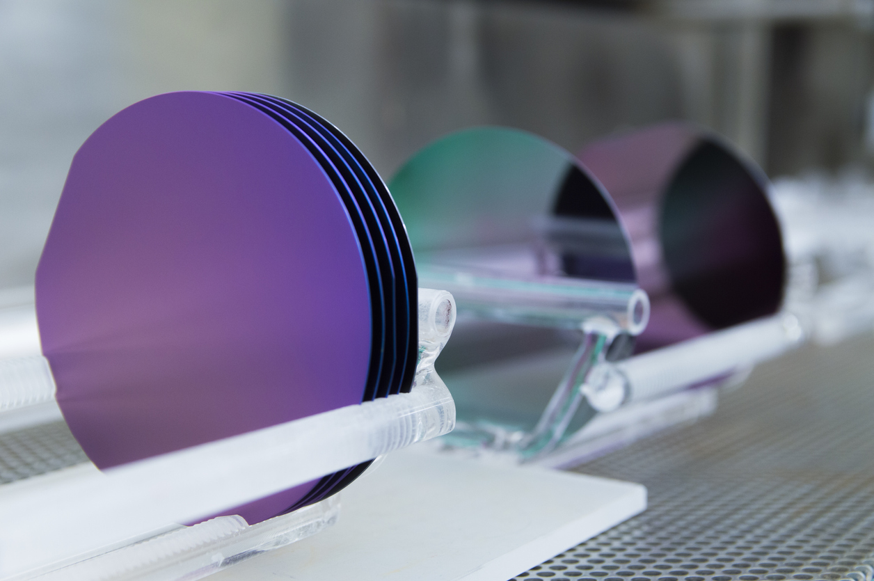
シリコンウェーハの研磨
表面スムースと平面化
研磨は表面を滑らかにし始めます, 準備する重要なステップ 半導体用シリコンウェーハ アプリケーション。 スライスプロセスから残っている不規則性に対処し始めます。 これは、溶融シリコンを金型に注ぐことで、カーフを除去し、均一な表面を確保します。 ウエハが冷やすと、平面層を取り除き、フラットベースを作成します.
表面をさらに磨き上げるために、界面活性剤溶液を塗布し、乾燥します。 表面欠陥を削減し、次の段階にウエハを用意します。 研磨液を使用して表面を円滑にします。 その後、ウエハを徹底的に洗い流して残りの界面活性剤を取り除きます。 これらのステップは、ウェーハが、高性能エレクトロニクスに必要な平坦性と円滑性を達成することを確認します.
鏡面仕上げを実現
最終的な磨くステップはウエファーをミラー様の表面に変形させます。 ウェーハの均一性と滑らかさを確保するのは、このプロセスが不可欠です。 ウェーハの表面からSOI(シリコンオン絶縁膜)フィルムを取り除き始めます。 次に平面研磨を行い、平面加工を行います。 このステップは、研磨スラリーでコーティングされた鋳鉄ラッピングプレートがウェーハとプレートの間に回転するウェーハラッピングを頻繁に使用します.
仕上げの接触のために、アルカリエッチング剤およびアンモナル安定させたコロイド無水ケイ酸のスラリーを含んでいる磨く解決は加えられます。 二重面研磨は、特に半導体製造のために、より均一な表面を達成するために推奨されます。 裏側でも作れるように、レオグラフィも行います。 これらの技術は、シリコンウェーハが現代の電子機器の厳しい要件を満たしていることを確認します.
ニンポー VET エネルギー技術Co.、 シリコンウェハを極端に精密・品質でお届けする高度な研磨技術を採用。 自社の専門知識により、あらゆるウェーハが達成されるようにします 鏡面仕上げが必要 最先端のアプリケーション用.
シリコンウェーハの洗浄・検査
汚染物質の除去
シリコンウェーハの洗浄 パフォーマンスを損なうことができる汚染物質を除去することが不可欠です。 これを実現するために複数の方法を使うことができます。 メタノールまたはアセトンによる溶剤洗浄などの洗浄技術は、有機不純物を効果的に排除します。 超音波風呂は頑固な粒子を分解することによってこのプロセスを高めます。 硫黄酸および過酸化水素を使用するRCAのクリーニングは、有機材料および金属のイオンを取除くための別の信頼できる方法です。 酸化ケイ素の層に対処するために、水溶性の酸のすくいはプリスチンの表面を保障します.
環境に優しい選択のために、レーザーのクリーニングのような乾燥したクリーニング方法は過度の化学薬品を使用しない汚染物質を取除きます。 これらの技術は、半導体アプリケーションに必要な高い基準を満たしながら、ウェーハの表面の完全性を維持します.
品質管理および欠陥の検出
クリーニングの後、シリコンウェーハを検査すると、厳格な品質基準を満たします。 高度な技術のような 光学検査システム 表面の欠陥および不規則性を検出して下さい。 X線および音響顕微鏡検査は、ウェーハの内部構造に非破壊的なインサイトを提供します。 電子顕微鏡検査(DR-SEM)による欠陥検査は、表面欠陥の高倍率解析を実現します.
機械学習によって動力を与えられる自動欠陥の分類は品質管理の効率を高めます。 このステップはウエハが物理的または電気的欠陥からミラーのような表面、自由に達成することを保障します。 厳格な検査基準を維持することで、現代の電子機器で使用するためのウェーハの信頼性を保証します.
ニンポー VET エネルギー技術Co.、 当社は、最先端洗浄技術を採用し、業界最高水準のシリコンウェーハを納入しています。 自社の専門知識により、あらゆるウェーハが最先端のアプリケーションに対応できるようにします.
シリコンウェーハの製造には、半導体アプリケーションにおける信頼性を確保するための一連の精密な手順が含まれています。 各段階は、浄化から検査まで、直接性能に影響を与えます.
- 表面平坦性は、フォトリソグラフィ精度を高めます, デバイス構造を定義するための重要な.
- 不純物制御は伝導性およびキャリアの可動性のような電気特性を改善します.
- 品質管理は一貫した性能および信頼性を保証します.
より大きいウエファーのサイズおよびウエファー レベルの包装のような高度の生産性および効率を可能にするより大きいウエファーのサイズおよびウエファー レベルの包装のような高度は現代電子工学に更に革命を起こしました。 このプロセスは、毎日頼る技術の背後にある複雑さを強調します.