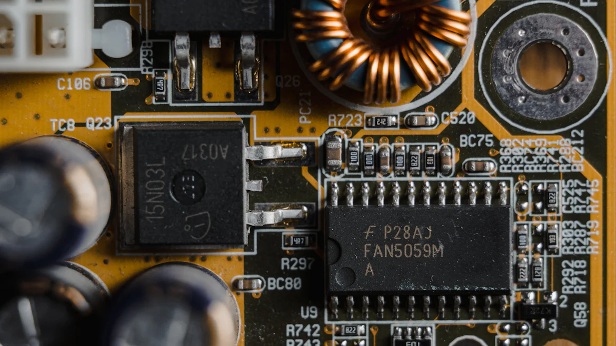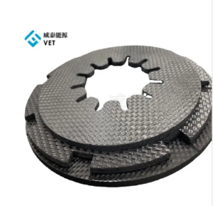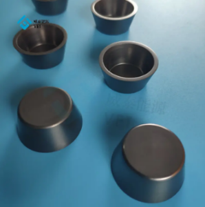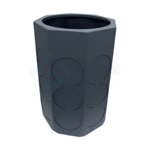
Rapid Thermal Processing (RTP) and Rapid Thermal Annealing (RTA) technologies have revolutionized semiconductor manufacturing. These methods enable precise thermal treatments, essential for creating advanced microchips. By delivering controlled heat to wafers, they ensure uniformity and accuracy in the fabrication process. The RTP/RTA carrier has become a cornerstone of innovation, driving progress in chip design and production. Its ability to meet the demands of smaller, more complex devices highlights its critical role in shaping the semiconductor industry.
Key Takeaways
- RTP and RTA technologies revolutionize semiconductor manufacturing by providing precise thermal treatments essential for advanced microchip production.
- The evolution from single-wafer to batch processing systems has significantly increased productivity, allowing multiple wafers to be treated simultaneously.
- Advanced temperature control mechanisms, such as pyrometers and infrared sensors, enhance the reliability of RTP/RTA processes, reducing defects and improving chip quality.
- Innovations in annealing methods and materials have enabled the production of smaller, high-performance chips, supporting the industry’s push towards miniaturization.
- The integration of AI and machine learning in RTP/RTA processes optimizes thermal cycles, leading to higher productivity and better-quality semiconductor devices.
- RTP and RTA technologies are crucial for supporting next-generation chip designs, including FinFET and 3D NAND architectures, which require precise thermal processing.
- As the semiconductor industry evolves, the RTP/RTA carrier will continue to play a vital role in meeting the demands of emerging technologies like AI and IoT.
The Origins of RTP/RTA Technology

Early Development and Applications
Emergence of RTP/RTA in the 1970s and 1980s
The semiconductor industry witnessed significant advancements during the 1970s and 1980s. Among these, the introduction of Rapid Thermal Processing (RTP) and Rapid Thermal Annealing (RTA) marked a turning point. Engineers developed these technologies to address the growing need for precise thermal treatments in chip manufacturing. Traditional methods struggled to meet the demands of emerging semiconductor designs. RTP and RTA offered a solution by delivering rapid and controlled heating to silicon wafers. This innovation allowed manufacturers to process materials with greater accuracy and efficiency.
The RTP/RTA carrier concept emerged as a critical enabler during this period. It provided a platform for handling wafers while ensuring uniform heat distribution. This approach minimized thermal stress and improved the quality of semiconductor devices. By the late 1980s, RTP and RTA had become essential tools in the production of advanced microchips.
Initial Use Cases in CMOS Technology and Semiconductor Processing
Complementary Metal-Oxide-Semiconductor (CMOS) technology became one of the first areas to benefit from RTP and RTA. These processes played a vital role in doping, oxidation, and annealing steps. Manufacturers used RTP to activate dopants in silicon wafers, which enhanced the electrical properties of transistors. RTA, on the other hand, proved effective in repairing damage caused by ion implantation. These applications improved the performance and reliability of CMOS devices.
Semiconductor processing also saw broader adoption of RTP and RTA techniques. The ability to achieve precise temperature control made these methods ideal for fabricating smaller and more complex devices. As the industry moved toward miniaturization, RTP and RTA became indispensable for meeting the stringent requirements of modern chip designs.
Overcoming Early Challenges
Limitations of Early Equipment and Processes
The initial versions of RTP and RTA equipment faced several limitations. Early systems lacked the ability to maintain consistent temperature profiles across wafers. This inconsistency often led to defects in the final products. Additionally, the equipment required frequent calibration, which increased downtime and reduced productivity. Engineers also struggled to develop materials that could withstand the high temperatures involved in these processes.
Despite these challenges, researchers continued to refine the technology. They introduced advanced heating systems and improved wafer carriers to enhance thermal uniformity. These innovations addressed many of the early limitations and paved the way for wider adoption.
Industry Skepticism and Gradual Adoption
The semiconductor industry initially approached RTP and RTA with caution. Many manufacturers doubted the reliability and scalability of these new processes. Traditional thermal methods had been in use for decades, and transitioning to a novel approach required significant investment. However, the growing demand for high-performance chips eventually drove the industry to reconsider.
Pilot projects demonstrated the potential of RTP and RTA to improve production efficiency and product quality. Leading companies began to adopt these technologies for specific applications, such as annealing and oxidation. Over time, the success of these implementations convinced others to follow suit. By the end of the 1980s, RTP and RTA had gained widespread acceptance as essential tools in semiconductor manufacturing.
Evolution of the RTP/RTA Carrier
Advancements in Equipment and Processes
Transition from single-wafer to batch processing systems
The semiconductor industry initially relied on single-wafer systems for RTP and RTA processes. These systems processed one wafer at a time, ensuring precise thermal control but limiting throughput. As demand for higher production volumes grew, manufacturers sought more efficient solutions. Batch processing systems emerged as a game-changer. These systems allowed multiple wafers to undergo thermal treatment simultaneously, significantly increasing productivity. Engineers designed these systems to maintain uniform heat distribution across all wafers, ensuring consistent quality. This transition marked a pivotal moment in the evolution of the RTP/RTA carrier, enabling it to meet the industry’s growing needs.
Integration of precise temperature control mechanisms
Temperature control plays a critical role in RTP and RTA processes. Early systems struggled to achieve consistent thermal profiles, leading to defects in semiconductor devices. To address this issue, engineers developed advanced temperature control mechanisms. Innovations such as pyrometers and infrared sensors allowed real-time monitoring of wafer temperatures. These tools ensured precise heating and cooling cycles, reducing the risk of thermal stress. The integration of these mechanisms enhanced the reliability of the RTP/RTA carrier, making it indispensable in modern semiconductor manufacturing.
Innovations in Materials and Techniques
Development of annealing methods for smaller nodes
As semiconductor devices became smaller, traditional annealing methods faced limitations. Engineers needed new techniques to address the challenges of shrinking node sizes. Advanced annealing methods, such as spike annealing and millisecond annealing, emerged as effective solutions. These methods delivered rapid and controlled heat pulses, minimizing diffusion and preserving the integrity of smaller features. The RTP/RTA carrier adapted to support these innovations, ensuring compatibility with cutting-edge processes. This development enabled manufacturers to produce high-performance chips with greater precision.
Use of advanced materials to enhance thermal uniformity
Thermal uniformity remains a key factor in the success of RTP and RTA processes. Early systems often experienced uneven heat distribution, which compromised device quality. To overcome this challenge, researchers introduced advanced materials for wafer carriers. Materials such as silicon carbide and quartz offered superior thermal conductivity and durability. These materials ensured even heat transfer across wafers, reducing defects and improving yield rates. The adoption of these materials further solidified the RTP/RTA carrier’s role as a cornerstone of semiconductor manufacturing.
Standardization and Industry Adoption
Adoption by leading semiconductor manufacturers
Leading semiconductor manufacturers recognized the potential of RTP and RTA technologies early on. Companies such as Intel and TSMC integrated these processes into their production lines to enhance chip performance. The RTP/RTA carrier played a crucial role in this adoption, providing the necessary infrastructure for efficient thermal processing. Its ability to deliver consistent results made it a preferred choice for high-volume manufacturing. This widespread adoption underscored the carrier’s importance in advancing semiconductor technology.
Establishment of global standards for RTP/RTA processes
The growing use of RTP and RTA technologies prompted the need for standardization. Industry organizations collaborated to establish global standards for these processes. These standards defined best practices for equipment design, temperature control, and material selection. The RTP/RTA carrier became a benchmark for compliance, ensuring uniformity across manufacturing facilities worldwide. Standardization not only improved process reliability but also facilitated collaboration among industry players. This milestone highlighted the carrier’s role in unifying the semiconductor industry.
Impact of RTP/RTA on Semiconductor Manufacturing

Enhancing Chip Design and Performance
Role in reducing defects and improving electrical properties
RTP and RTA technologies have significantly improved the quality of semiconductor devices. By delivering precise thermal treatments, these processes reduce defects in silicon wafers. Defect reduction enhances the structural integrity of chips, ensuring better performance and reliability. The controlled heating and cooling cycles also optimize the electrical properties of transistors. This optimization results in faster switching speeds and lower power consumption, which are critical for modern electronic devices.
Contribution to scaling down transistor sizes
The semiconductor industry continuously strives to create smaller and more efficient transistors. RTP and RTA have played a pivotal role in this effort. These technologies enable precise annealing processes that support the fabrication of smaller nodes. As transistor sizes shrink, maintaining performance becomes increasingly challenging. RTP and RTA address this challenge by ensuring uniform thermal processing, which preserves the functionality of miniaturized components. This contribution has been instrumental in advancing Moore’s Law and enabling the production of high-density chips.
Boosting Production Efficiency
Faster processing times and reduced energy consumption
Manufacturers rely on RTP and RTA to streamline production processes. These technologies offer rapid thermal treatments, significantly reducing processing times compared to traditional methods. Faster processing allows manufacturers to meet high demand without compromising quality. Additionally, RTP and RTA systems consume less energy due to their efficient heating mechanisms. Lower energy consumption not only reduces operational costs but also aligns with sustainability goals in semiconductor manufacturing.
Lower manufacturing costs and higher yields
The adoption of RTP and RTA has led to cost savings in chip production. Precise thermal control minimizes material waste and reduces the likelihood of defects. Fewer defects translate to higher yields, which directly impacts profitability. The RTP/RTA carrier ensures consistent results across multiple wafers, further enhancing production efficiency. These benefits make RTP and RTA indispensable tools for cost-effective semiconductor manufacturing.
Enabling Next-Generation Technologies
Support for FinFET, 3D NAND, and advanced architectures
Emerging chip architectures demand advanced manufacturing techniques. RTP and RTA have proven essential for technologies like FinFET and 3D NAND. These architectures require precise thermal treatments to achieve the desired electrical properties. RTP and RTA processes ensure uniformity and accuracy, which are critical for these complex designs. The RTP/RTA carrier provides the necessary infrastructure to handle these advanced architectures, supporting innovation in chip design.
Contribution to AI, IoT, and other emerging applications
The rise of artificial intelligence (AI) and the Internet of Things (IoT) has created new demands for semiconductor technology. RTP and RTA enable the production of chips that power these applications. By enhancing chip performance and efficiency, these processes support the development of AI processors and IoT devices. The ability to produce high-performance chips at scale positions RTP and RTA as key drivers of technological progress in these fields.
Current Trends and Future Outlook for RTP/RTA Carriers
Recent Innovations in RTP/RTA Technology
Integration of AI and machine learning for process optimization
The integration of artificial intelligence (AI) and machine learning (ML) has transformed the capabilities of RTP and RTA technologies. Engineers now use AI algorithms to analyze vast amounts of process data in real time. These algorithms identify patterns and optimize thermal cycles with unmatched precision. Machine learning models predict potential issues before they occur, reducing defects and improving yield rates. This proactive approach enhances the efficiency of the RTP/RTA carrier, making it a vital tool for modern semiconductor manufacturing.
AI-driven systems also enable adaptive control during thermal processing. Sensors collect data on wafer temperature and heat distribution. The system adjusts parameters instantly to maintain uniformity and prevent overheating. This level of control ensures consistent results across production lines. By leveraging AI and ML, manufacturers achieve higher productivity and better-quality chips.
Development of ultra-fast and energy-efficient annealing techniques
Recent advancements have introduced ultra-fast annealing methods that significantly reduce processing times. Techniques like flash annealing and laser-based annealing deliver rapid heat pulses to wafers. These methods minimize thermal diffusion, preserving the integrity of smaller nodes. The RTP/RTA carrier supports these innovations by providing a stable platform for precise heat delivery.
Energy efficiency has also become a priority in annealing processes. Engineers have developed systems that consume less power while maintaining high performance. Improved heating mechanisms and advanced materials contribute to this efficiency. These developments align with the industry’s sustainability goals, reducing the environmental impact of semiconductor manufacturing.
Future Directions in Semiconductor Manufacturing
Applications in emerging materials like 2D semiconductors
The rise of 2D semiconductors, such as graphene and transition metal dichalcogenides, has opened new possibilities for chip design. These materials offer exceptional electrical and thermal properties, making them ideal for next-generation devices. RTP and RTA processes play a crucial role in integrating 2D materials into semiconductor manufacturing. Precise thermal treatments ensure the stability and functionality of these materials during fabrication.
The RTP/RTA carrier adapts to handle the unique requirements of 2D semiconductors. Its ability to provide uniform heat distribution supports the delicate nature of these materials. As research progresses, the carrier will continue to enable breakthroughs in 2D semiconductor applications.
Role in supporting next-generation chip designs and architectures
Next-generation chip architectures demand advanced manufacturing techniques. Technologies like gate-all-around (GAA) transistors and 3D stacking require precise thermal processing. RTP and RTA systems meet these demands by delivering controlled heat treatments that enhance device performance. The RTP/RTA carrier ensures compatibility with these complex designs, enabling seamless integration into production lines.
Future chip designs will also focus on higher efficiency and lower power consumption. RTP and RTA processes contribute to these goals by optimizing electrical properties and reducing defects. As the industry moves toward more innovative architectures, the RTP/RTA carrier will remain a cornerstone of semiconductor manufacturing.
RTP and RTA technologies have undergone a remarkable transformation, shaping the semiconductor industry’s history. Their evolution highlights their critical role in advancing chip manufacturing processes. The RTP/RTA carrier has consistently driven innovation, enabling manufacturers to meet the demands of modern microchip designs. Its contributions to precision, efficiency, and scalability underscore its importance in the industry. Continued advancements in these technologies will remain essential as the semiconductor sector tackles future challenges and explores emerging applications. The RTP/RTA carrier will undoubtedly continue to serve as a foundation for progress in this ever-evolving field.


